





2026-08-26
Board-to-Board Connector Types for Reliable Industrial Control Cabinets
View More


 FPC/FFC Connector
Board to Board Connector
Wire to Board Connector
Flexible Flat Cable
RF Connector
I/O Header
FPC/FFC Connector
Board to Board Connector
Wire to Board Connector
Flexible Flat Cable
RF Connector
I/O Header
Product
Automotive
Product
 141091-211260
 Consult

Compact automotive ECUs place much greater demands on internal interconnects than simply fitting two PCBs together. A reliable automotive board-to-board connector strategy must account for the ECU’s mechanical stack-up, vibration exposure, temperature movement, high-speed channel performance, power loading, PCB manufacturability, and module-level validation.
Connector selection should begin with the ECU architecture—not with pitch, pin count, or a catalog drawing.
A compact ECU may combine a processor, memory, PMIC, power stage, communication interfaces, sensor interfaces, external I/O, and thermal-management features within one restricted enclosure. In these systems, the board-to-board connector becomes part of the module architecture because it affects board spacing, enclosure dimensions, assembly flow, signal routing, grounding, and serviceability.
Typical multi-PCB ECU configurations include:
Parallel stacked PCBs for domain controllers and gateways
Perpendicular PCBs in constrained control modules
Separate processor, I/O, and power boards
Communication boards handling Ethernet, camera, RF, or vehicle-network functions
Display, HMI, or camera-processing boards in smart cockpit systems
For example, a domain controller may place the MCU or SoC, memory, and communication processing on an upper board while locating power distribution and external interfaces on a lower board. The connector must then provide a defined stacking height while leaving room for shielding, airflow, thermal pads, mechanical supports, and assembly tooling.
Before selecting an automotive board-to-board connector, define:
Available PCB footprint and keep-out area
Board-to-board distance and maximum ECU height
Required signal, ground, and power contact count
Highest data rate and interface type
Continuous and peak-current demand
Enclosure temperature range
Vibration, shock, and thermal-cycling conditions
PCB fixing method, support-post locations, and enclosure datum strategy
SMT process, mating direction, inspection access, and rework needs
Customer validation requirements and target service life
A connector that fits the schematic may still be the wrong choice if it creates an unstable mechanical stack-up or an impractical production process.
The nominal mating height in a connector drawing is only one variable. In a compact ECU, the actual distance and alignment between two boards can vary due to PCB thickness tolerance, board warpage, solder-joint height, connector coplanarity, housing flatness, mounting-hole position, support-post height, screw loading, fixture accuracy, and thermal expansion.
A robust design evaluates X, Y, and Z positional tolerance as well as angular variation. PCB or connector position deviation can create side loading and forced mating. Board-spacing variation can lead to incomplete engagement or over-compression. PCB rotation, bending, or uneven support can create uneven contact loading and solder-joint stress.
The risk rises when two or more rigid board-to-board connectors connect the same PCB pair. Even small positional deviations can accumulate. One connector may mate normally while another is forced sideways during assembly, transferring stress into the connector housing, contacts, PCB pads, or solder joints.
A floating board-to-board connector is useful when the assembly must accommodate controlled positional variation between boards. Its floating mechanism can help compensate for X/Y and, depending on the product design, limited Z-direction variation caused by assembly tolerance, vibration, or thermal movement.
In applications where fixed board positioning is difficult to maintain throughout assembly and vehicle operation, connector compliance becomes an important part of the mechanical-reliability strategy. This is especially relevant in high-density assemblies that combine tight packaging constraints with vibration exposure and repeated thermal expansion.
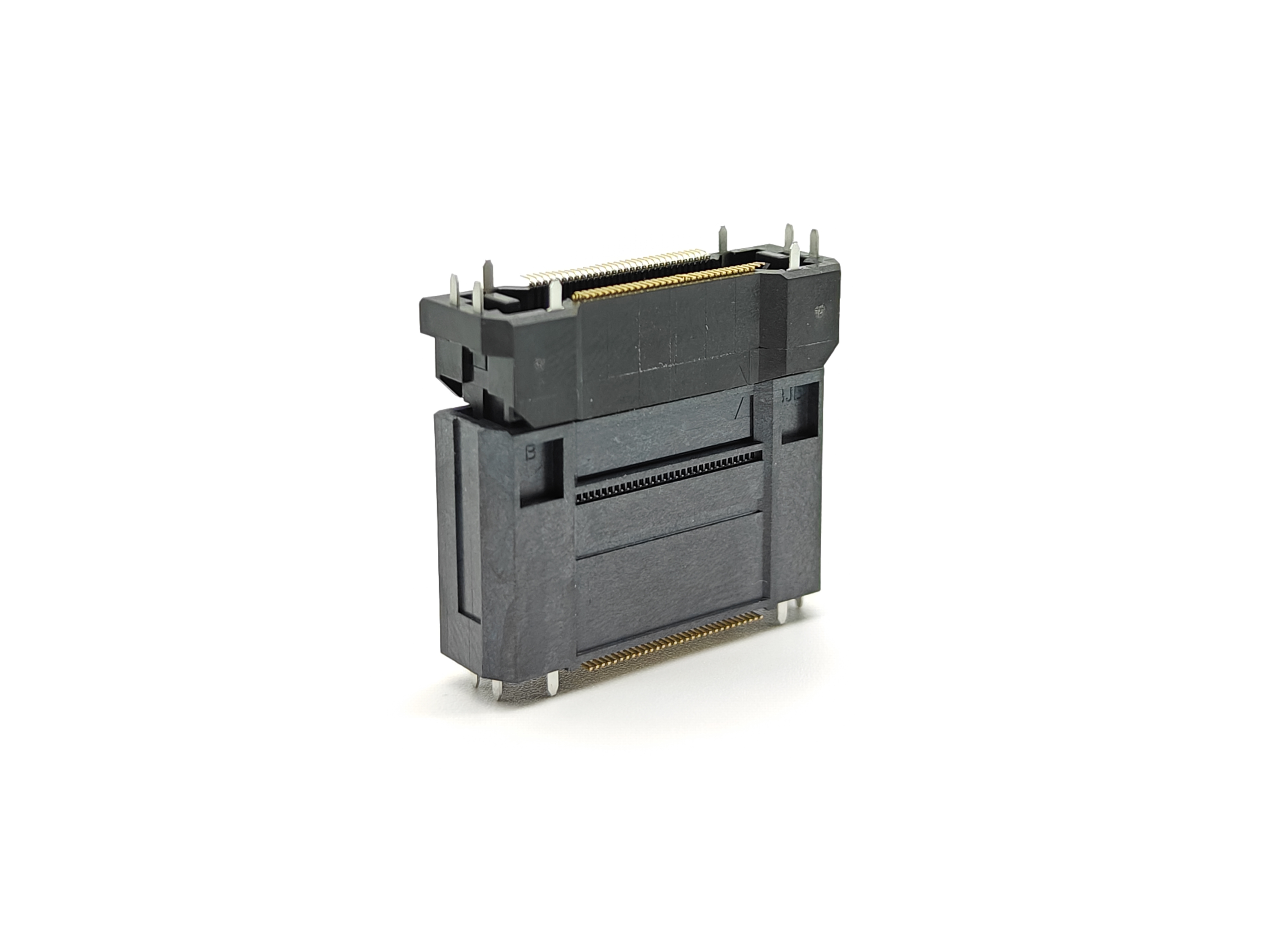
Within this application context, BJD floating board-to-board connectors are designed for high-density automotive electronics such as new-energy-vehicle domain controllers, smart cockpit modules, and LiDAR-related assemblies. These applications may benefit from controlled positional compensation when PCB assembly tolerance, vibration stress, and thermal movement must be managed.
Important: A floating design can help improve assembly yield and reduce stress caused by slight misalignment, but it is not a substitute for sound mechanical design. The connector should not carry the primary structural load of the module.
Use screws, locating pins, support posts, enclosure ribs, brackets, and controlled datums to limit PCB bending and relative motion.
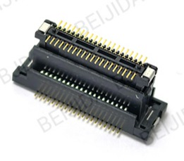
In a compact ECU, the connector may carry high-speed differential signals, low-speed control signals, analog sensing, power distribution, and ground return paths. These should be evaluated as one electrical system rather than as separate pin-count requirements.
For high-speed interfaces, the connector is part of the complete transmission channel between the two PCBs. That channel includes PCB traces, via transitions, connector contacts, and the transition into the second PCB.
The complete channel can introduce impedance discontinuities, insertion loss, return loss, skew, crosstalk, and common-mode noise. These effects become increasingly important in processors, cameras, displays, telematics, gateways, and ADAS-related electronic architectures.
Key design practices include:
Maintain differential impedance across both PCBs and the connector transition
Use continuous reference planes for return current
Assign nearby ground contacts to high-speed signal groups where the connector design supports it
Avoid routing differential pairs across split planes
Control trace width, spacing, via structure, and pair-length matching
Separate sensitive analog signals from high-current and switching-noise contacts
Review connector pin assignment for crosstalk and return-path continuity
Run SI simulation before layout release
Validate the full channel with appropriate TDR, insertion-loss, return-loss, eye-diagram, BER, or functional tests
Once the required interface, channel budget, and board-to-board mechanical tolerance have been defined, engineers can compare connector systems against the ECU’s actual data-rate, impedance, pin-assignment, power-delivery, shielding, and signal-integrity requirements. The comparison should be based on full-channel performance—including PCB traces, vias, connector transitions, and return paths—rather than on a nominal data-rate claim alone.
This is particularly important in dense multi-board modules, where the connector may need to support high-speed differential links, power delivery, and controlled positional compensation at the same time. For example, BJD’s 0.5-8 High-speed Transmission Floating Series supports PCIe Gen4 and a transmission rate of up to 16 Gbps, with an 85 Ω differential-impedance specification. Its 0.5 mm pitch design is available in 20 to 160 pin positions and stacking heights from 10 to 30 mm.
The series also provides XY floating capability of ±0.8 mm to help accommodate controlled PCB-position variation during assembly. In addition, its hybrid architecture combines signal contacts rated at 0.5 A per pin with four power terminals rated at up to 6 A per pin. These characteristics make it a connector series that engineers can evaluate for compact, high-density internal interconnect applications where high-speed channel performance, power loading, and assembly tolerance need to be considered together.
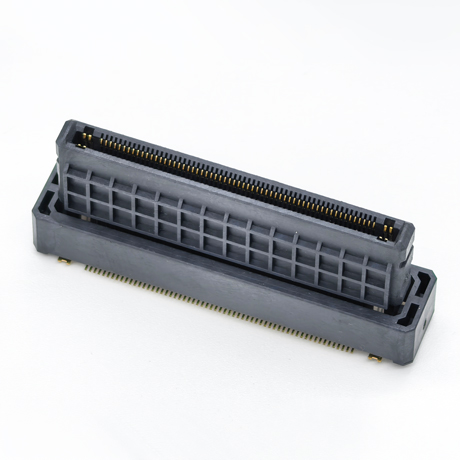
Power-contact selection should be based on actual operating conditions, not only the nominal current value in a product specification. Current capability is affected by enclosure temperature, adjacent powered contacts, trace resistance, copper thickness, airflow, connector pitch, contact resistance, and long-term thermal aging.
For higher-current functions:
Evaluate power-contact temperature rise under realistic loading
Consider multiple parallel contacts only when allowed by the connector design
Route parallel contacts symmetrically to support current sharing
Include voltage-drop testing under continuous and peak loads
Keep heat-generating switching components away from fine-pitch connector areas
Reserve adequate ground contacts for return current, noise control, and shielding performance
Ground pins are not unused capacity. They help control return-current paths, reduce noise, improve signal quality, and support system-level EMC performance.
A well-selected connector can still create quality problems if the PCB footprint and assembly process are not controlled. For fine-pitch automotive board-to-board connectors, layout quality, solder-paste design, component placement, and reflow consistency directly influence long-term reliability.
Use the manufacturer’s approved footprint, including land pattern, solder-mask opening, paste aperture, placement orientation, and keep-out area. Review these items during PCB layout and DFM:
Pad geometry and solder-mask clearance
Stencil thickness and paste-volume control
Surface finish and copper thickness
Via placement and solder-wicking risk
Via-in-pad filling and capping requirements
Connector coplanarity requirements
Pick-and-place nozzle clearance
Reflow profile compatibility
AOI and X-ray inspection access
Mechanical clearance for mating and module assembly
Avoid placing high-power inductors, large capacitors, hot semiconductors, or high-current switching loops immediately beside a fine-pitch BTB connector. Excess localized heat can contribute to board warpage, contact-resistance growth, material aging, and EMI coupling.
A practical zoning approach separates high-speed digital circuits, power-conversion circuits, sensitive analog circuits, communication interfaces, and connector-transition areas. This makes it easier to protect return paths, manage thermal flow, preserve inspection access, and reduce coupling between noisy power circuits and sensitive signal channels.
A connector datasheet is necessary, but it is not sufficient evidence of ECU reliability. The final validation sample should include the actual PCB materials, footprint, enclosure, support posts, screws, shielding, thermal pads, representative external loads, and final mating method.
Recommended module-level validation includes:
Random vibration and mechanical shock
Thermal cycling and thermal shock
High- and low-temperature storage
Temperature-humidity cycling
Mating and unmating durability
PCB bending and enclosure-distortion evaluation
Contact-resistance monitoring before and after environmental exposure
Power-contact temperature-rise and voltage-drop testing
Solder-joint inspection after environmental tests
Differential impedance, insertion loss, return loss, and crosstalk testing
Eye-diagram, BER, or functional communication tests where applicable
EMI/EMC evaluation with representative grounding and shielding conditions
Common failure modes include incomplete mating from tolerance accumulation, solder-joint cracking from PCB flexure, vibration-induced contact instability, fretting corrosion from micro-motion, temperature rise at power contacts, signal degradation from poor pin assignment, and EMI problems caused by interrupted return paths.
The most effective prevention is a cross-functional design review involving hardware, PCB layout, mechanical engineering, SI/EMC, reliability, and manufacturing before the design is released.
For compact automotive ECUs, the board-to-board connector is a system-level design decision rather than a simple PCB-to-PCB interface. Selecting the correct architecture, managing the tolerance stack-up, protecting signal and return-current paths, controlling thermal loading, and validating the real module can improve assembly yield, electrical performance, vibration reliability, and long-term vehicle operation.