





2026-08-26
Board-to-Board Connector Types for Reliable Industrial Control Cabinets
View More


 FPC/FFC Connector
Board to Board Connector
Wire to Board Connector
Flexible Flat Cable
RF Connector
I/O Header
FPC/FFC Connector
Board to Board Connector
Wire to Board Connector
Flexible Flat Cable
RF Connector
I/O Header
Product

Automotive
Product
 141091-211260
 Consult

Modern commercial LED displays are expected to deliver finer pixel pitch, thinner cabinets, higher refresh performance, and faster module replacement—all while fitting more electronics into less space. For display manufacturers, the interconnect strategy is therefore no longer a minor PCB detail. It directly affects module yield, cabinet thickness, service efficiency, electrical stability, and long-term reliability.
High-density board-to-board connectors provide a practical way to connect LED lamp boards, HUB boards, receiving cards, power boards, and control PCBs in compact display assemblies. When selected around the actual mechanical, electrical, and manufacturing requirements, they can reduce connector footprint, simplify routing, and make multi-board assemblies more tolerant of real-world production variation.
For LED display designers, the key question is not simply “How many pins are needed?” It is how to achieve stable power and signal transmission while allowing for PCB tolerance, thermal movement, assembly speed, and repeated module service.
A commercial LED display module contains far more than LEDs. Depending on the application, the internal architecture may include LED lamp boards, driver ICs, HUB boards, receiving cards, power-distribution circuits, scan boards, control PCBs, and structural mounting parts.
As pixel pitch decreases, designers must place more driver circuits, capacitors, routing channels, and interconnects within the same—or a smaller—PCB area. This creates a combination of electrical and mechanical design pressures:
Limited PCB space for connectors, driver ICs, capacitors, and copper routing
Multiple PCB interfaces that must mate accurately during module assembly
Tolerance accumulation from PCB fabrication, housing dimensions, fasteners, and fixtures
Mechanical stress caused by rigid mating interfaces
Signal degradation risks in dense layouts
Current-density and temperature-rise concerns in compact power paths
Faster front-service or rear-service module replacement requirements
Traditional pin headers can still be suitable for straightforward designs. However, when a module needs several simultaneous mating points, a thinner stack-up, or tighter production tolerances, a conventional rigid connector may introduce unnecessary assembly risk.
This is where high-density board-to-board connectors become part of the display architecture rather than just a component-selection exercise.
A board-to-board connector creates a direct electrical connection between two PCBs. Depending on the enclosure design, it can support parallel stacking, vertical mating, right-angle connection, or blind mating inside a cabinet.
High-density board-to-board connectors typically combine fine contact pitch, a compact footprint, higher pin count, surface-mount compatibility, and low-profile mating structures. Their value in LED display design comes from enabling more signal, ground, and power connections within limited board area.
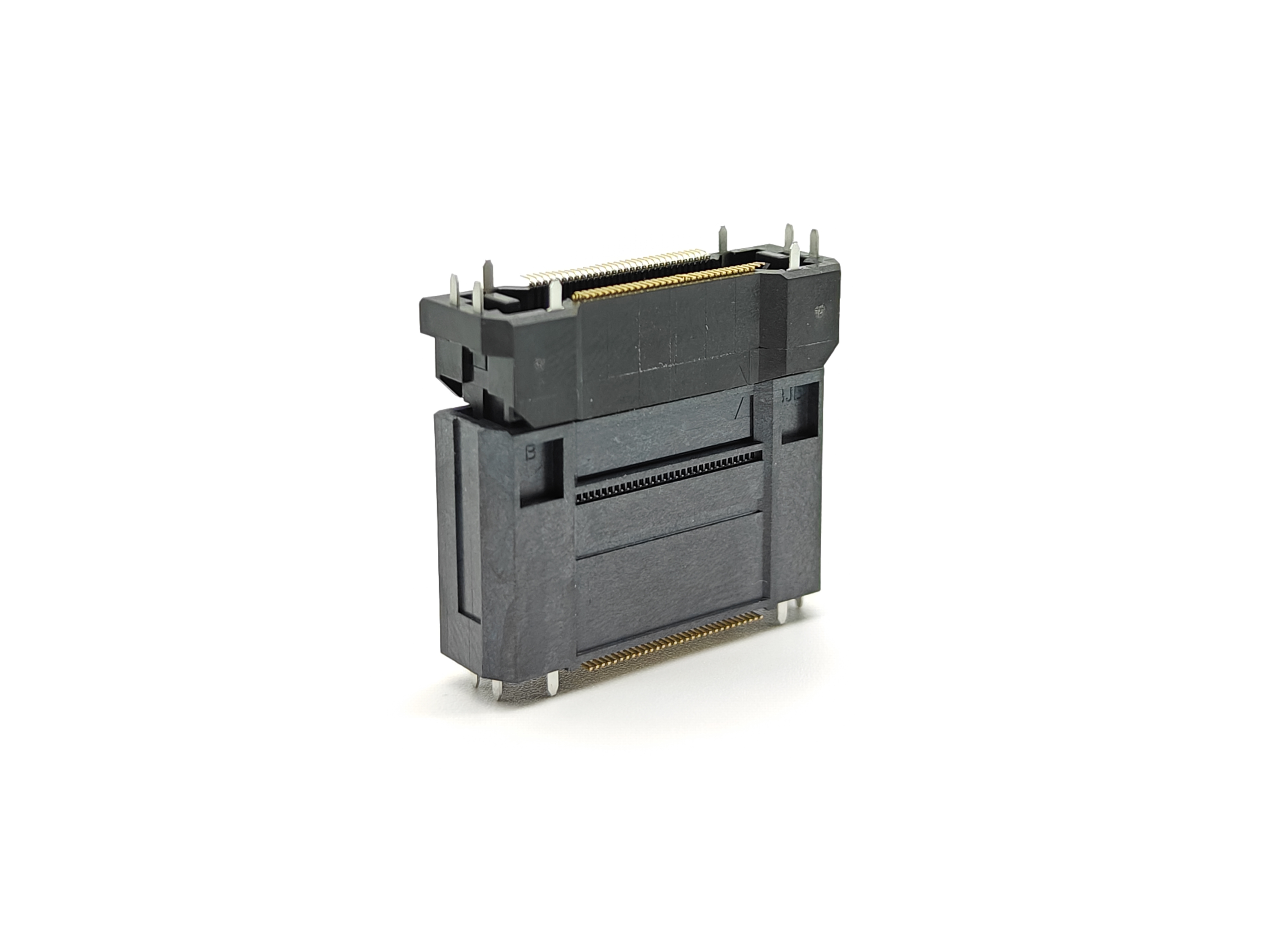
BJD’s board-to-board connector portfolio includes floating and high-speed series with 0.5 mm, 0.635 mm, and 0.8 mm pitch options. Available configurations include pin counts from 20 to 160 positions, selected power-terminal options, SMT mounting, and specified floating ranges for tolerance compensation.
A high-density interface can help designers:
Consolidate power, ground, data, control, and detection connections
Reduce the number of separate connector interfaces
Lower module thickness through compact stacking structures
Release PCB area for LED driver and signal-routing requirements
Reduce wire-harness complexity inside the display cabinet
Support modular PCB replacement and more repeatable assembly
However, density alone should not determine the connector choice. The smallest pitch is not automatically the best solution. Pitch, stacking height, mating tolerance, power demand, service cycles, signal type, and production capability must be evaluated together.
One of the biggest assembly risks in LED display modules is accumulated positional variation. Even when every individual PCB and mechanical part meets its drawing tolerance, several interfaces may not align perfectly once they are installed inside the same module.
A conventional rigid board-to-board connector requires close alignment during mating. If the boards are shifted by enclosure tolerance, mounting-hole variation, fixture positioning, or multiple mating points, forced insertion can create stress on contacts, connector housings, and solder joints.
A floating board-to-board connector is designed to absorb a defined amount of positional movement after mating. This capability is especially relevant for compact LED modules with multiple PCBs or blind-mating structures.
BJD’s floating connector range includes options with XY floating capability from ±0.5 mm to ±0.8 mm; B0813 series configuration specifies XY ±0.5 mm and Z ±0.8 mm movement. Rather than treating this movement as a general performance guarantee, engineers should match the specific connector’s published range with their calculated worst-case assembly tolerance.
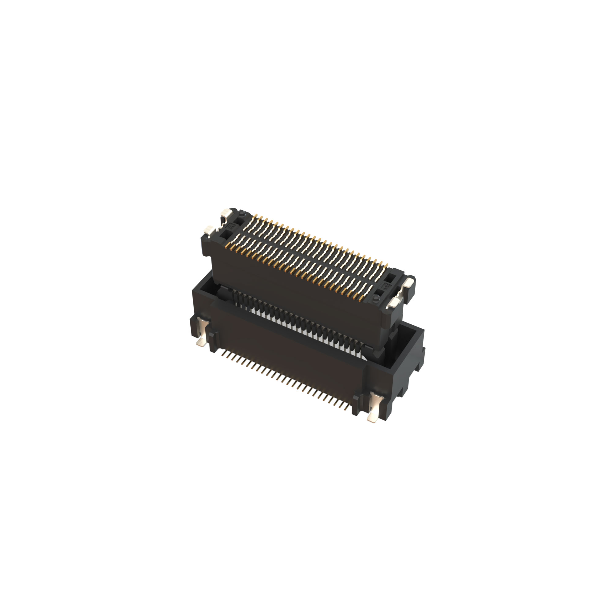
In LED display assembly, a floating design can help compensate for controlled mating offset, reduce accumulated tolerance pressure when multiple connectors engage together, and lower the chance of forced or uneven insertion during repetitive module installation. It can also help reduce stress transferred to contacts and solder joints when vibration, structural movement, or thermal expansion affects the board position.
For LED display manufacturers, this can contribute to smoother assembly and a lower risk of connector damage or inconsistent mating during production. The practical benefit is not only electrical continuity; it is a more robust module assembly process.
Fine-pitch LED displays place high demands on PCB real estate. The connector footprint competes with LED drivers, decoupling capacitors, thermal structures, mounting holes, power routing, and signal channels.
High-density board-to-board connectors can improve this layout efficiency by placing more contacts in a compact interface. But an aggressive pitch choice can also increase SMT-process sensitivity, inspection difficulty, and rework risk.
The right connector selection should consider:
PCB fabrication and assembly capability
Solder-paste printing accuracy
Pick-and-place precision
Optical inspection coverage
Rework accessibility
Mating-force requirements
Connector coplanarity and solder-joint reliability
Field replacement frequency
For higher-integration applications, designers may also need a connector that supports both signal and power functions. BJD’s 0.5 mm high-speed floating series, for example, lists 20 to 160 positions, four power terminals, 6 A per power terminal, 0.5 A per signal pin, 10–30 mm stacking heights, and up to 16 Gbps transmission capability for the specified series.
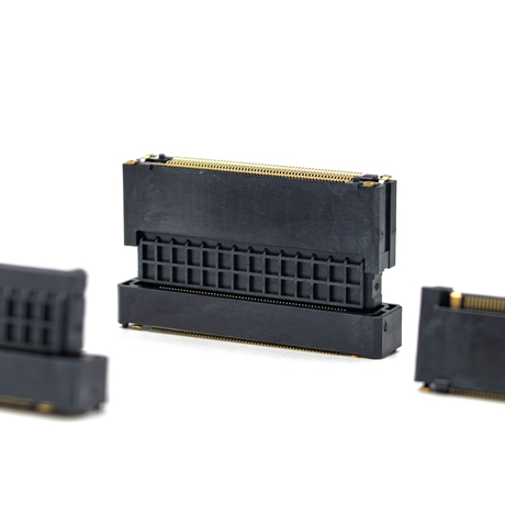
These figures should be treated as series-specific reference parameters—not as a substitute for system-level validation. In particular, actual current capability depends on the number of energized adjacent contacts, PCB copper design, ambient temperature, mating condition, ventilation, and load profile.
LED display modules may not always use the same data rates as computing equipment, but signal integrity remains important as scan performance, refresh rates, grayscale requirements, and module density increase.
Connector selection and pin assignment should be considered as part of the complete electrical path between the control circuitry and the LED driver network.
Keep critical signal paths between the connector and driver ICs short
Provide continuous and intentional ground-return paths
Separate sensitive signals from high-current or noisy power paths
Use appropriate differential-pair routing where the interface requires it
Review via placement, impedance discontinuities, and stack-up design
Avoid treating connector pin assignment as an afterthought
A connector rated for high-speed transmission does not automatically guarantee good system-level signal performance. PCB layout, return-path continuity, trace geometry, grounding strategy, and nearby switching noise all influence the result.
Power-contact selection should begin with the real display load profile, not only the nominal current rating in a catalog. LED brightness, scan duty cycle, thermal conditions, and the number of simultaneously energized power contacts can significantly affect connector temperature rise and voltage drop.
A practical power-design review should include:
Required current for the operating display mode
Number of power and ground contacts in parallel
Contact resistance and voltage-drop budget
Trace width, copper thickness, and current-path length
Cabinet airflow and local temperature conditions
Connector derating under adjacent loaded contacts
Temperature-rise testing under realistic load conditions
This type of analysis helps reduce the risk of uneven brightness, excessive connector heating, unstable power delivery, and long-term contact degradation.
Not every LED display interconnect should use direct board-to-board mating. In some module designs, boards are offset, need to fold, or require a flexible path around mechanical structures. In these cases, an FPC/FFC connector architecture may be more suitable.
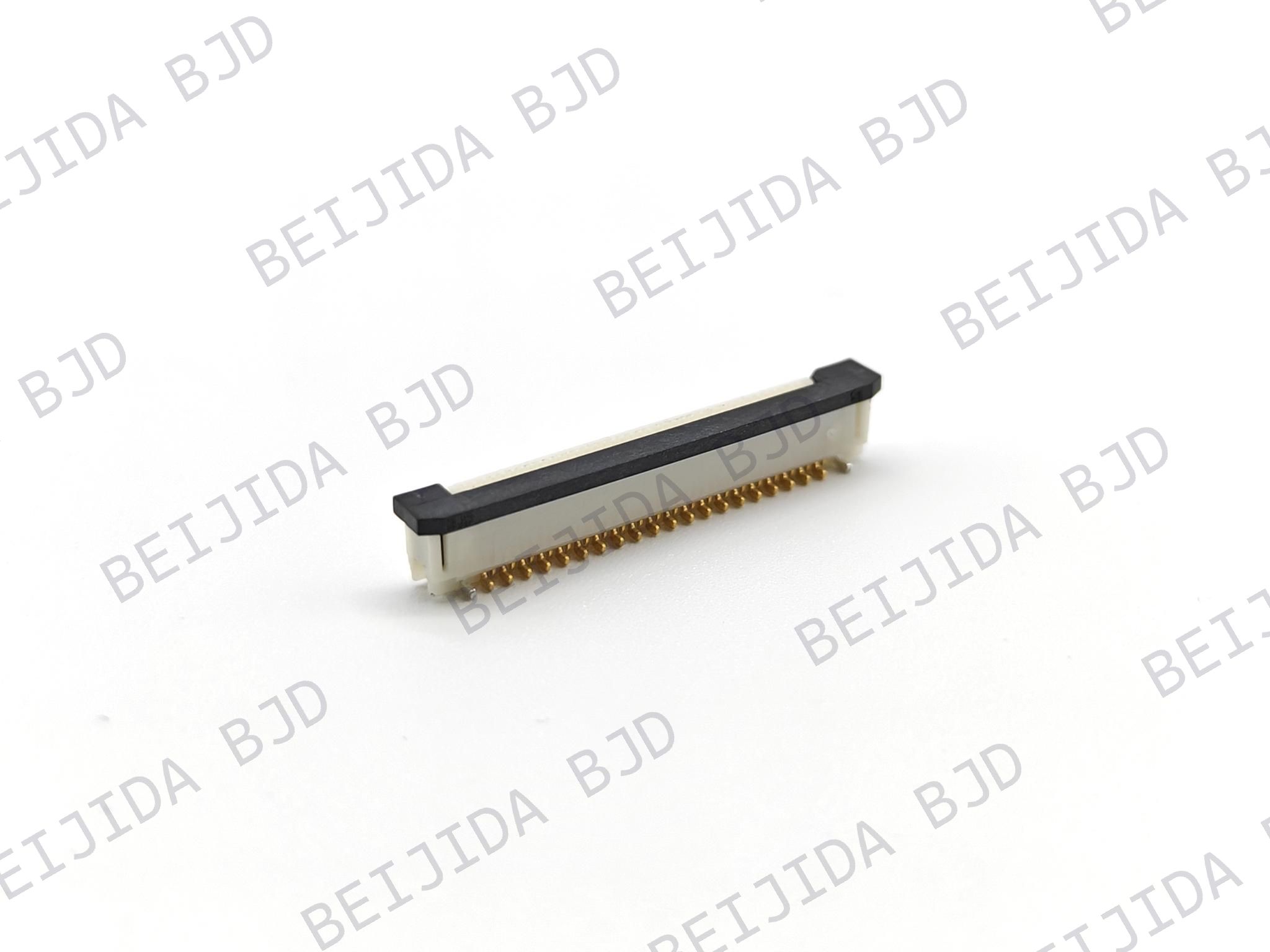
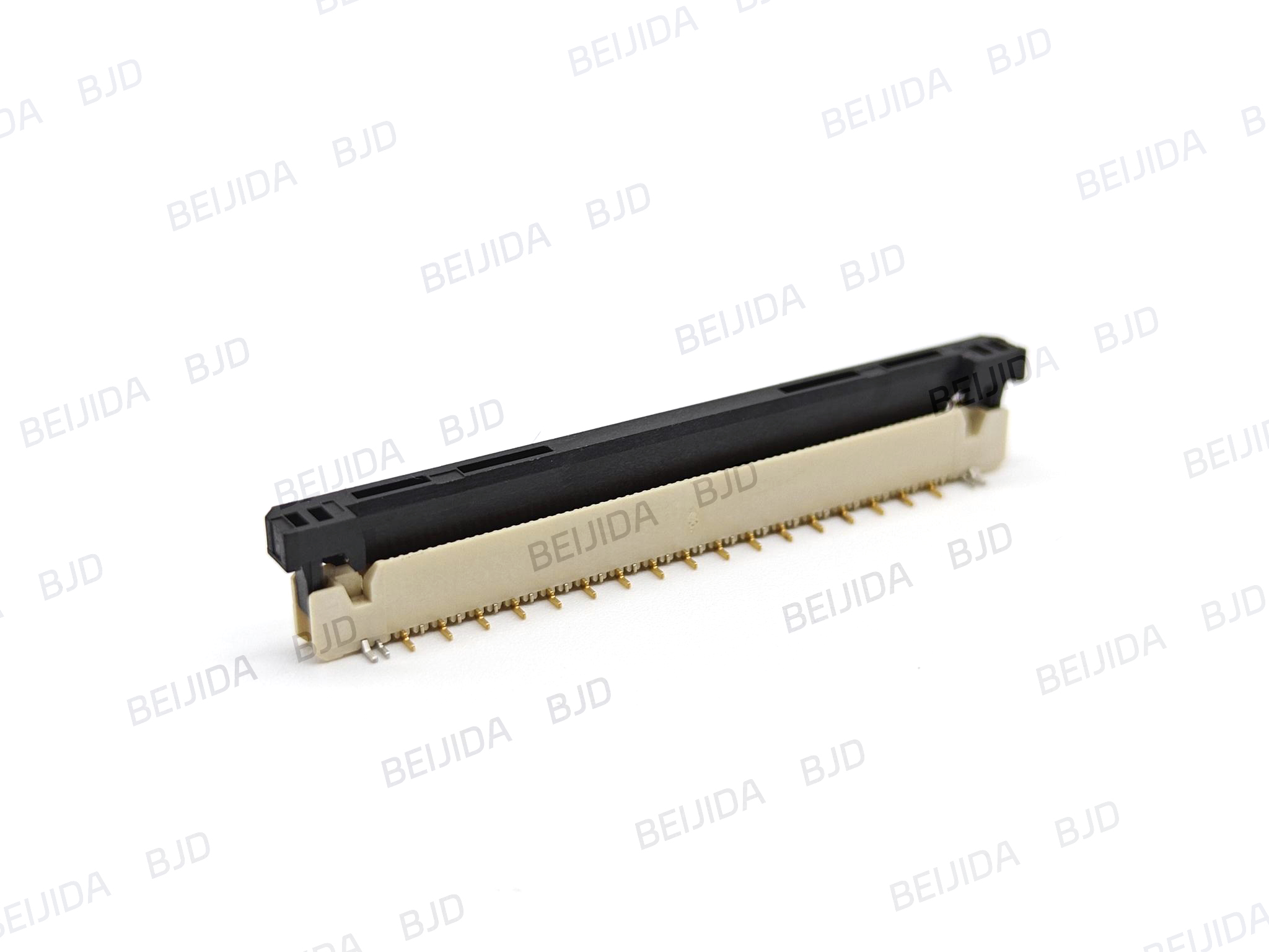
BJD’s FPC/FFC connector portfolio includes 0.4 mm, 0.5 mm, and 1.0 mm pitch options; product configurations include ZIF and non-ZIF designs, horizontal and vertical SMT mounting, multiple locking mechanisms, and pin-count options that extend to 120 positions in the catalog filters.
For LED display equipment, FPC/FFC interconnects can be considered when:
PCBs cannot mate directly because of mechanical offset
A flexible cable must fold within a constrained module space
The connection crosses non-parallel boards
The assembly needs a lightweight alternative to a conventional wire harness
Service access requires routing flexibility
For compact direct mating between fixed parallel PCBs, a high-density board-to-board connector is usually appropriate. When several mating points, blind mating, or tolerance accumulation are involved, a floating board-to-board connector may be more suitable. For flexible routing between offset or foldable assemblies, FPC/FFC connectors can provide the required routing freedom. Where high-current paths must be combined with compact signal interfaces, designers should choose a connector series with suitable dedicated power contacts and validate it at the system level.
Instead of starting with a preferred pitch or part number, LED display teams should start with a system requirement map.
Clarify whether the boards are parallel, vertical, right-angle, blind-mated, front-service, or rear-service. Establish the available stacking height and the mechanical support arrangement before narrowing down connector families.
List every required connection, including power, ground, LED-driving signals, data, control lines, detection pins, shielding or ground references, and future-reserved positions.
Include PCB dimensions, mounting holes, housing tolerances, fasteners, fixtures, module frames, and the number of simultaneous mating points. If the result approaches the connector’s alignment limit, assess a floating design early.
Estimate worst-case current, select appropriate power and ground allocation, and test voltage drop and temperature rise under representative operating conditions.
Evaluate SMT capability, inspection, mating accessibility, insertion force, rework, and module replacement frequency. A connector that works in a prototype may not be the best option for high-throughput production.
Testing should cover more than initial electrical continuity. Recommended validation may include contact resistance, mating and unmating force, repeated mating cycles, thermal cycling, powered temperature-rise testing, humidity exposure, vibration, mechanical shock, solder-joint inspection, and worst-case misalignment tests.
Connector performance is strongly connected to the quality of the development and validation process behind it. For applications involving compact multi-board structures, design teams benefit from suppliers that can support mechanical tolerance review, structural analysis, signal-integrity considerations, and application-specific customization.
BJD, established in 2004, develops connector solutions across board-to-board, floating board-to-board, FPC/FFC, wire-to-board, high-frequency/RF, and I/O header product lines. Its company information describes high-tech enterprise and provincial specialized-and-sophisticated enterprise qualifications, a CNAS-certified laboratory, independent design and development capability, automated production processes, and technical capabilities including mold-flow, CAE structural, and signal-integrity analysis.
Although BJD’s core business experience is rooted in automotive electronics, its connector solutions are also positioned for industrial equipment, commercial LED displays, medical devices, security equipment, energy storage, robotics, and other high-integration electronic applications. This cross-application experience is relevant to LED display projects because display modules face many similar engineering concerns: dense PCB packaging, vibration, thermal cycling, repeated service operations, and the need for reliable compact interconnects.
For a new LED display platform, the most effective time to involve a connector supplier is before the PCB outline, stacking height, and mounting approach are finalized. Early technical review can identify avoidable issues in pin assignment, tolerance stack-up, mating access, and power-path allocation before tooling and mass-production commitments are made.
High-density board-to-board connectors can help LED display manufacturers create thinner, more integrated, and more serviceable modules. Their greatest value comes from addressing the complete interconnect challenge: PCB space, alignment tolerance, signal routing, power delivery, thermal behavior, production yield, and field maintenance.
For multi-PCB LED modules, a floating connector design deserves particular attention when several interfaces must mate at once or when blind assembly is required. For fixed direct board connections, a high-density compact BTB interface may offer the most efficient layout. For offset or foldable structures, FPC/FFC solutions can provide needed routing flexibility.
The best connector is not simply the smallest option or the one with the highest pin count. It is the interface that matches the actual display architecture and has been validated for its electrical load, mechanical tolerance, assembly process, and service life.
Explore BJD connector solutions for board-to-board, floating board-to-board, and FPC/FFC interconnection requirements, and assess connector architecture early in the LED display design process.